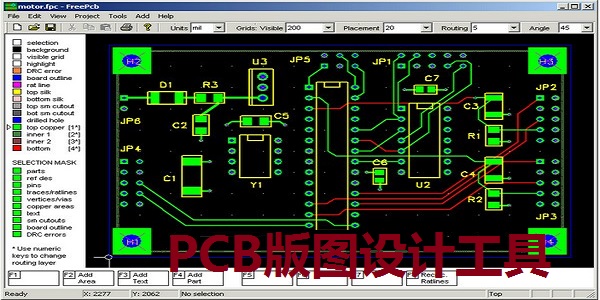
PCB layout design tool (FreePCB) software functions
1. Supports 1 to 16 copper layers
2. The size of the circuit board can reach 60 inches × 60 inches
3. Most functions use imperial or metric units (i.e. mils or millimeters)
4. The footprint library is provided by Ivex Design International, PCB Matrix and IPC
5. Copper filled area
6. Footprint Wizard and Footprint Editor are used to create or modify footsteps
7. Import and export PADS-PCB netlist
8. Export extended Gerber files (RS274X) and Excellon drill files
9. Design Rule Checker
10. Automatically save
PCB layout design tool (FreePCB) software features
Most functions work in imperial or metric units (i.e. milliliters or millimeters).
Trail Wizard and Trail Editor to create or modify trails
Import and export pads-pcb netlist
Export extended Gerber files (rs274x) and Excellon drill files
Instructions for use of PCB layout design tool (FreePCB)
1. If you use FreePCB to design your PCB, I highly recommend checking your Gerber files with a program like ViewMate (available for free here) before spending any money on making your board.
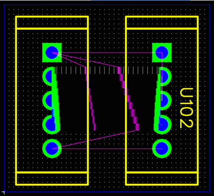
2. These libraries are from the new IPC-7351 standard for SMT pad patterns. They are from PCB Libraries LP Created from data extracted from Viewer (version 6.20.00).
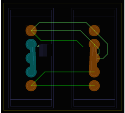
3. Three different pad sizes are provided, minimum, nominal and maximum (i.e. small, medium and large).
4. If you use these libraries, I highly recommend downloading the LP Viewer application from the PCB library (now called PCB Matrix, I think).
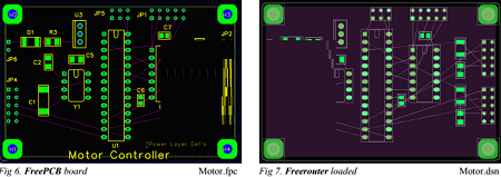
5. Using the viewer, you can browse and search the library, providing excellent graphical and dimensional information for each component and land pattern.
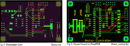
6. Then, you can easily find the corresponding package in the FreePCB library from the name and description.
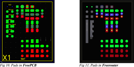
7. Gerbers generated by pads now use the pad shape and size specified in the footprint. The previous behavior was to ignore internal pad values and add circular pads as needed, based on the CAM pad minimum ring size value. These "dummy" pads are only added to Gerbers tracking when connected to Gerbers, otherwise they are omitted. The new behavior is to use pad to specify whether it is connected to a trace or not. If the pad shape is , the old virtual pad behavior specified as None will still be used.
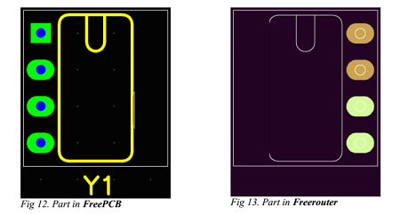
8. All pad shapes flash. Before this version, some pad shapes did not flash and were drawn as polygon files in Gerber. All non-basic shapes are now defined using the aperture macro and flash as needed.
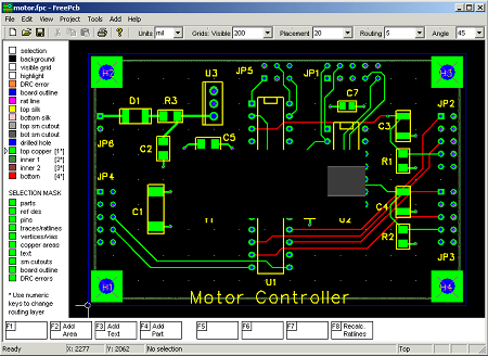
Comparison of similar software
Pad2PadIt is a general PCB circuit design software that provides easy-to-draw part tool production solutions and automatic wiring tools. Download Pad2Pad now and make your own printed circuit board
ADIsimPEIt is a circuit simulation software launched by ADI. It is mainly used for analog and mixed-signal circuit design and development. It has rich ADI IC model and application schematic library, accurate/verified IC models and circuit behavior.
Huajun editor recommends:
PCB layout design tool (FreePCB)It has a massive component library, so you don’t have to worry about finding power symbols. It supports one-click measurement and one-click preview. Interested students can quickly come to this site to download and use it!





it works
it works
it works