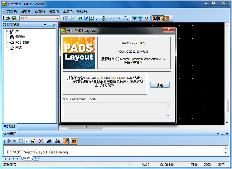
PADS LayoutSoftware introduction
Mentor Graphics PADS As the mainstream PCB design platform in the industry, the Layout/Router environment has been widely used in the most active industrial fields such as communications, semiconductors, consumer electronics, and medical electronics due to its powerful interactive layout and routing functions and ease of learning and use. . PADS Layout/ Router supports a complete PCB design process, covering the import of schematic netlist, rule-driven interactive layout and routing, DRC/DFT/DFM verification and analysis, until the final production file (Gerber), assembly file and bill of materials (BOM) output and other comprehensive functional requirements ensure that PCB engineers can complete design tasks efficiently.
PADS LayoutFunction introduction
PADS SPICEnet:
Export SPICE netlist files from PADS Logic. For SPICE simulation software to import simulation. Such as Intusoft ICAP/4, Berkeley SPICE 3.PSpice.
PADS Logic PDF:
Support for exporting smart holographic PDFs in PADS Logic document. All design information such as schematic hierarchical structure, component names and attributes, network name attributes, etc. are retained and can be browsed in PDF files.
Spice integration:
Export standard Spice netlist files from DxDesigner.
Variant Manager for PADS:
The derivation management module of the production material table supports the derivation of production material tables of different specifications from a PCB design to meet the needs of product preparation and processing of different grades and models. PCB can be set Options such as whether different components are installed or not, replacement models, etc.
PCB Editor:
Basic PCB design module, including manual layout and routing, design rule verification (DRC), manual copper laying, engineering modification command (ECO), pad and via library editing, Gerber Data output and other functions.
PADS Logic:
Schematic design environment. The following functions can be achieved
- Creation and editing of multi-page/hierarchical schematics
- Single/combined (Slot) schematic symbol creation and editing, providing a symbol wizard to help designers quickly create schematic symbols for multi-pin devices
-PCB netlist output, schematic and PCB interactive positioning (Cross Probe)
- Schematic diagram and PCB forward/backward annotation (Forward/Backward Annotation)
-Chinese character input
- Design Rule Check (DRC)
- PCB design rule definition, and the design rules can be exported to the PCB design environment along with the netlist
- Design report (BOM)
DxDesigner 040:
Schematic design and data management environment. The following functions can be achieved
- Creation and editing of multi-page/hierarchical schematics
- Create and edit single/combined (Slot/Fructure) schematic symbols, and provide symbol wizards to help designers quickly create schematic symbols for multi-pin devices. Pin and attribute information can be read from the Internet or device manuals provided by manufacturers, and standard schematic symbols can be automatically created.
-PCB netlist output, schematic and PCB interactive positioning (Cross Probe)
- Schematic diagram and PCB forward/backward annotation (Forward/Backward Annotation)
-Chinese character input
- You can search components (or networks) based on name, attributes and other information. Package preview function allows you to view the appearance, size and other information of the physical package used in schematic symbols.
- Design reuse
- Design Rule Check (DRC)
- PCB design rule definition, and the design rules can be exported to the PCB design environment along with the netlist
- The holographic archiving function can export design files to PDF documents. All design information such as schematic hierarchy, component names and attributes, network name attributes, etc. can be browsed in PDF files.
- Design report (BOM)
PADS LayoutSoftware features
1: Highlight the same worthy components in Pads layout.
2: Output patch images and gerber files
3: Groups of equal lengths in pads layout
4: Check the network length in pads router
5: Production of schematic package
6: Create a multi-part component.
7: Production of special-shaped pads
8: Some properties of pads logic display components
9: pads import dxf file
10: Display the filling of the copper skin of the keepout layer as a grid
11: Add ground vias
12: Properties of display components in pads logic
13: PADS LOGIC export BOM
14: How to disperse the components when importing the netlist in pads layout
15: pads layout rotates multiple components as a whole
16: The same schematic diagram is packaged in pcb and expressed in different pcb packaging forms
17: Hide the flying line of a certain network
18: Some traces (hollow ones) in the layout cannot be deleted, or they are via holes. Some components cannot be deleted because they are not locked, or there may be traces connected to the components that are locked.
19: Modified how to update the package into the pcb
PADS Layout update log
1. The pace of optimization never stops!
2. More little surprises are waiting for you to discover~
Huajun editor recommends:
Don’t miss it when you pass by. If you miss PADS Layout, you will never experience such a good service again. This site also recommends to youHaochen CAD,Yaochuang CAD,Huiyi CAD,vray for 3dmax2015,Quick CAD viewing software


it works
it works
it works